AI Is Changing How Semiconductor Fabs Work — and Engineers Are Moving Faster Because of It
Nov 3, 2026, 8:00 AM · NVIDIA Blog
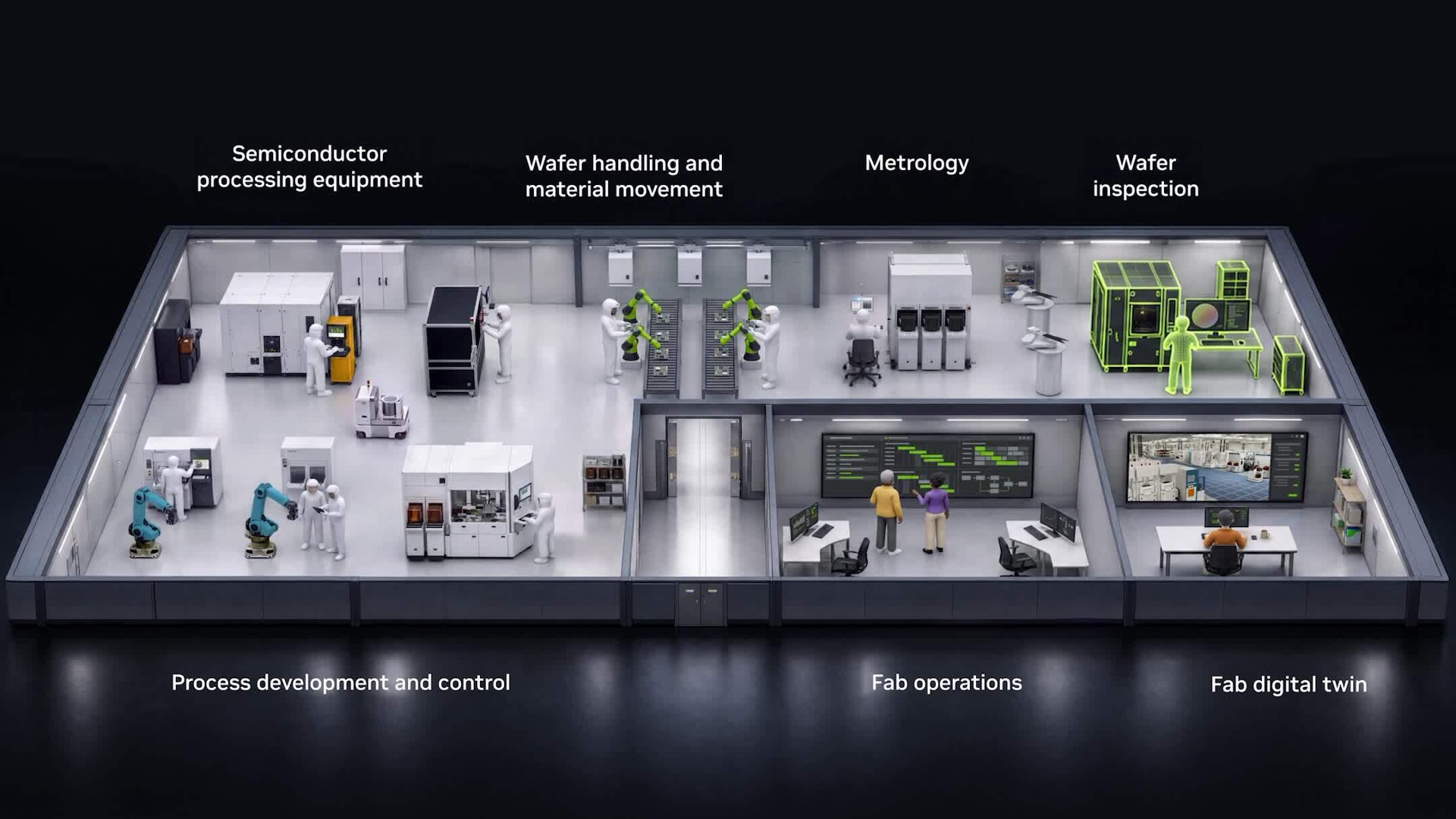
NVIDIA's pitch for the AI-defined fab is mostly partner speedups, and the useful parts are real, but this is a vendor describing a market it sells into.
Why it matters
Chipmaking is getting harder while demand rises. Engineers often wait days for simulations, and physical trials on a fab line are slow and expensive. NVIDIA's argument is that accelerated simulation, physics-trained AI models, agents and digital twins compress that waiting.
The post leans on partner claims. COMSOL and Applied Materials report up to 10x faster simulation with NVIDIA's cuDSS library. Applied's ACE+ platform reportedly runs topography simulations up to 35x faster with PhysicsNeMo. Siemens says cuLitho gives up to 17x on key lithography workloads. Lam Research showed plasma behavior predicted in milliseconds instead of days for a full simulation.
If those gains translate to the line, more alternatives get tested before anyone touches a wafer.
From the desk
We're broadly in favor of where this goes. Fabs are exactly the kind of place where cheaper, faster prediction pays off, because the alternative is burning real wafers and real time. A surrogate model that predicts plasma behavior in milliseconds lets engineers explore conditions they would never have paid days of compute to try.
But read this for what it is. It's an NVIDIA blog post, every number is an upper bound and nearly every example is a partner integrating NVIDIA libraries. There are no yield figures, no error bars on the learned physics models, and no discussion of when the fast prediction disagrees with the slow simulation. In manufacturing, a confident wrong answer can be worse than a slow right one.
The agent example is the thinnest. Advantest uses NeMo Switchyard agents to automate choosing which AI model to apply on the test floor, cutting response times from hours to minutes. That's welcome, but it's agents picking models, not agents running the fab.
We do appreciate that the framing keeps engineers in charge: they direct the work and make the calls. The trajectory to watch is the "connected loop," where production data feeds models that evaluate changes. That can make fabs learn faster. It also concentrates more of the industry's core tooling on one vendor's stack, which is a strategic risk for chipmakers that already depend on NVIDIA as a customer and supplier.
Context
Computational lithography determines how circuit patterns are printed onto silicon and is too compute-heavy to run on CPUs at production scale. Applied Materials uses NVIDIA Omniverse libraries to build digital twins of entire fabs, simulating material flow, bottlenecks, layouts and operating strategies before changes reach the floor.
Who feels it
- Process and yield engineers
- Faster simulation and learned surrogates mean more what-if exploration before physical trials.
- Chipmakers and equipment makers
- More of the toolchain, from simulation to digital twins, is converging on NVIDIA libraries, raising dependency questions.
- EDA and simulation vendors
- GPU acceleration is becoming table stakes, as COMSOL, Siemens and Applied integrations show.
What to watch
- Any partner disclosure tying these speedups to measured yield or cycle-time gains on production lines.
- Validation data on how often physics-trained surrogates diverge from full simulation.
- Whether agents move beyond model selection into process adjustment, and with what human sign-off.